 Geneva group March 2001
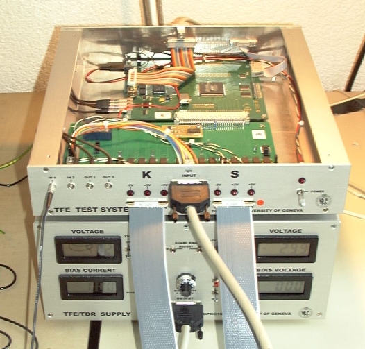
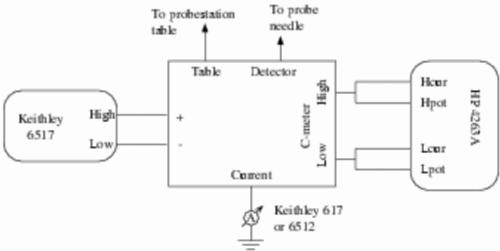
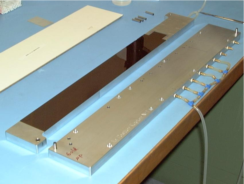
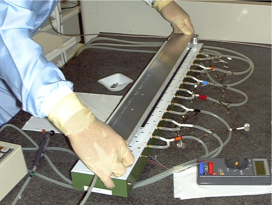
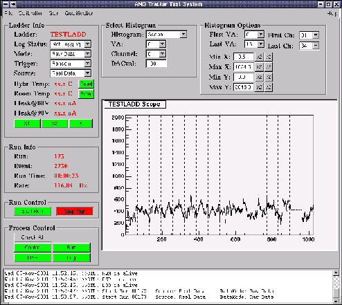 Tracker ground support equipment

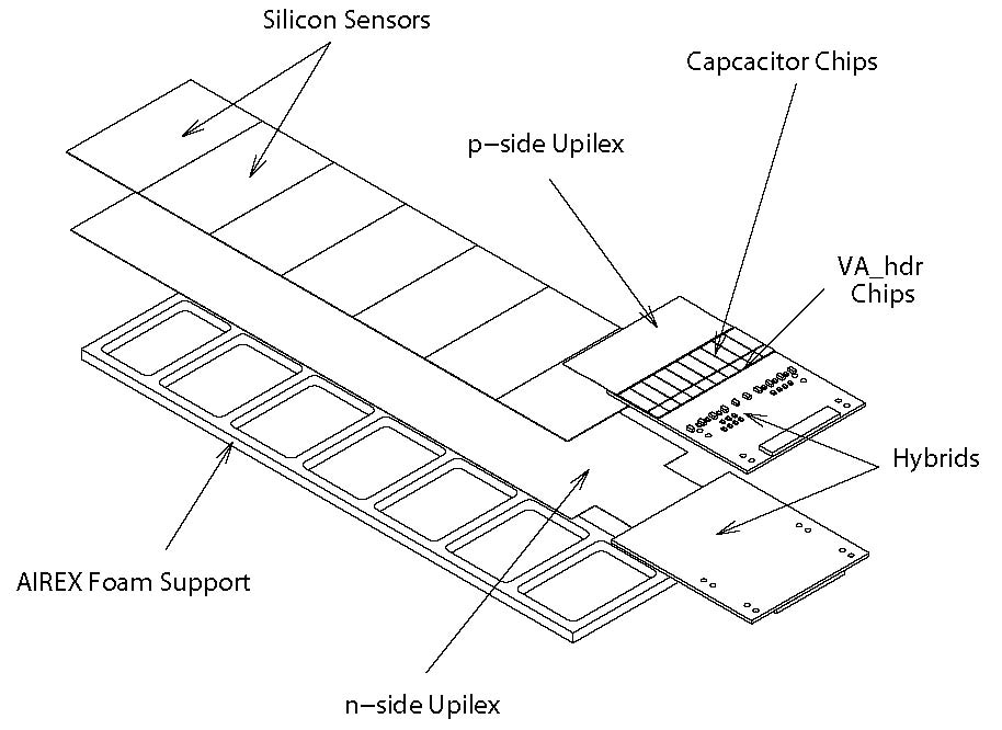
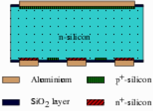 Silicon detector structure (PA fig. 3.13-3.16)
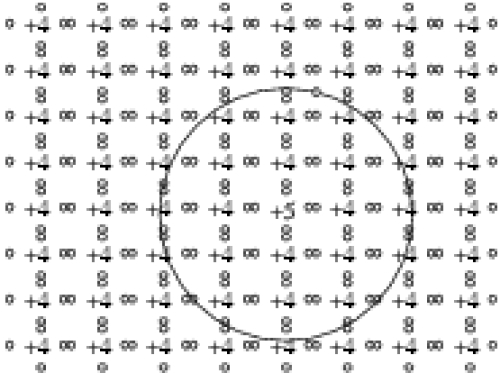
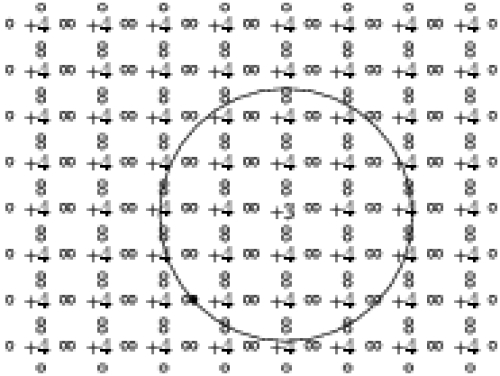
 n/p-doped Si (PA fig. 3.2-3.5)

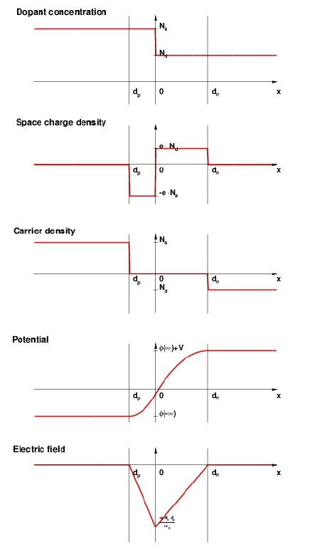

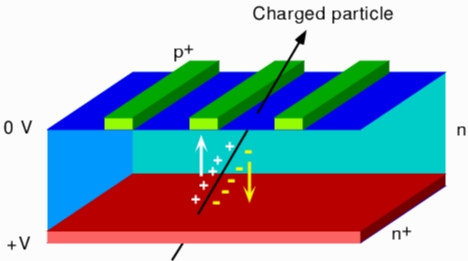
 p-n junction (PA fig. 3.7-3.10)
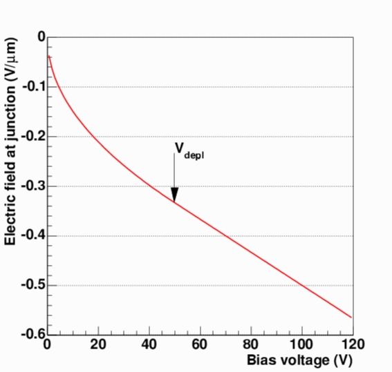
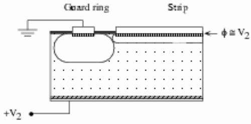
 Field and depletion width at p+nn+ junction (PA fig. 3.11, 3.12)

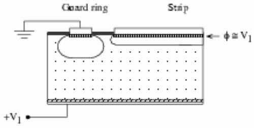
 Punch through method (PA fig. 3.17-3.20)
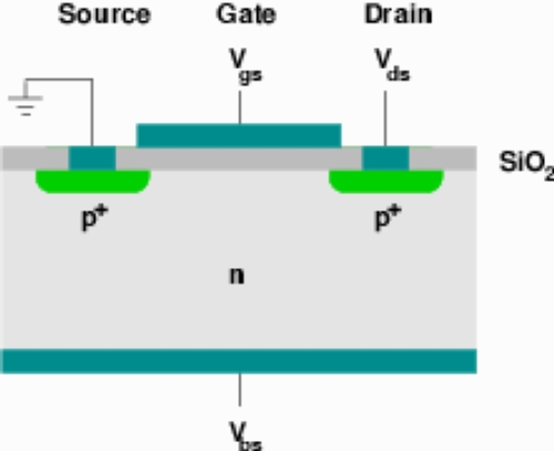

 MOSFET and FOXFET (PA fig. 3.12-3.24

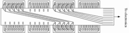 AMS daisy chaining (PA fig. 3.25, 4.9)
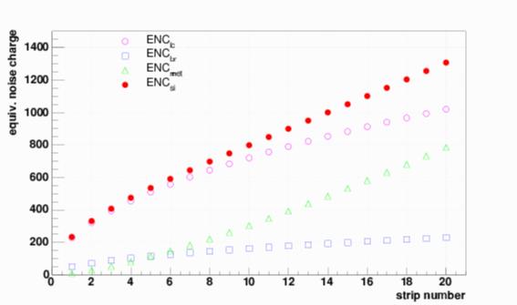
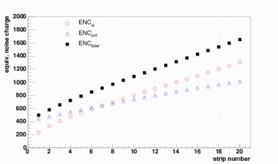
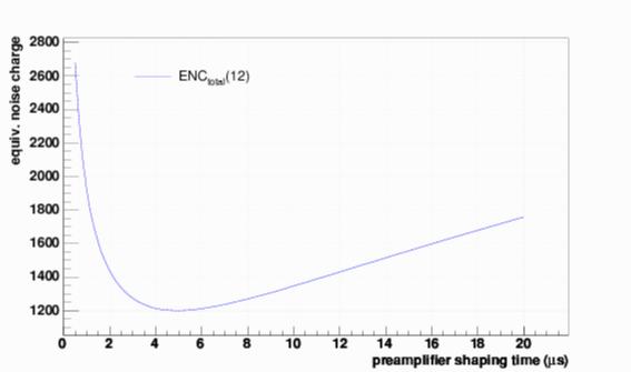 Noise contributions (PA fig. 3.31-3.33)

 AMS-01 and AMS-02 sensors (PA fig. 4.3)

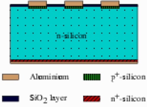
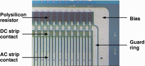
 Sensor metalization and structure (NIM fig. 2.58, PA fig. 5.1)

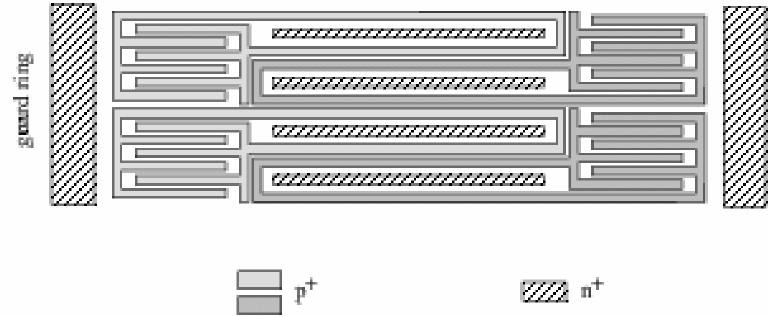
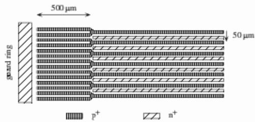
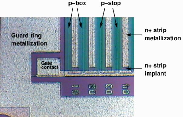 Gate and p-stop (PA fig. 4.4-4.6)
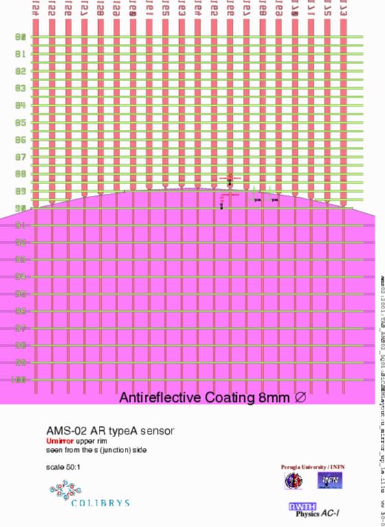
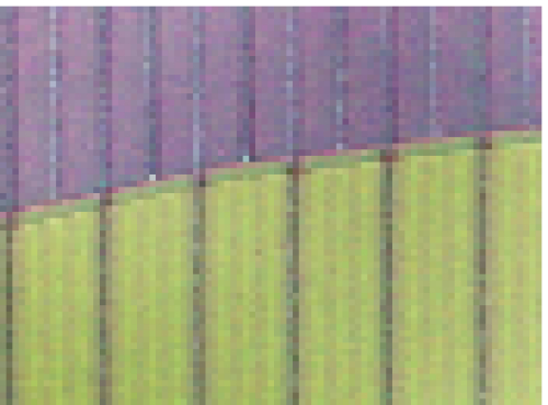
 Antireflective sensors (PA fig. 4.7, 4.8)


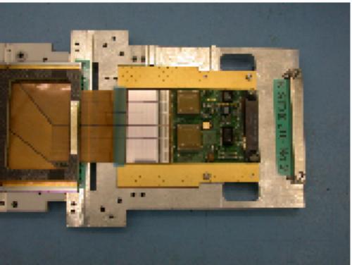
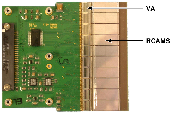 Front end hybrids (PA fig. 4.13, 4.14)
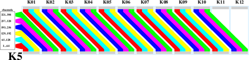
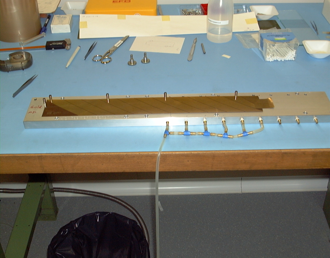
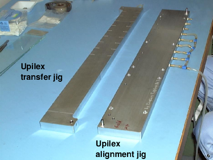
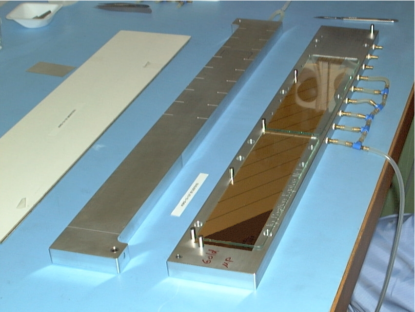
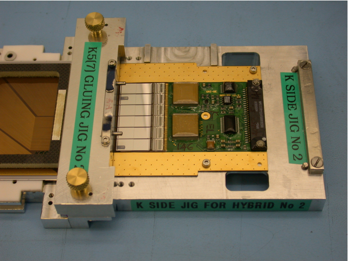
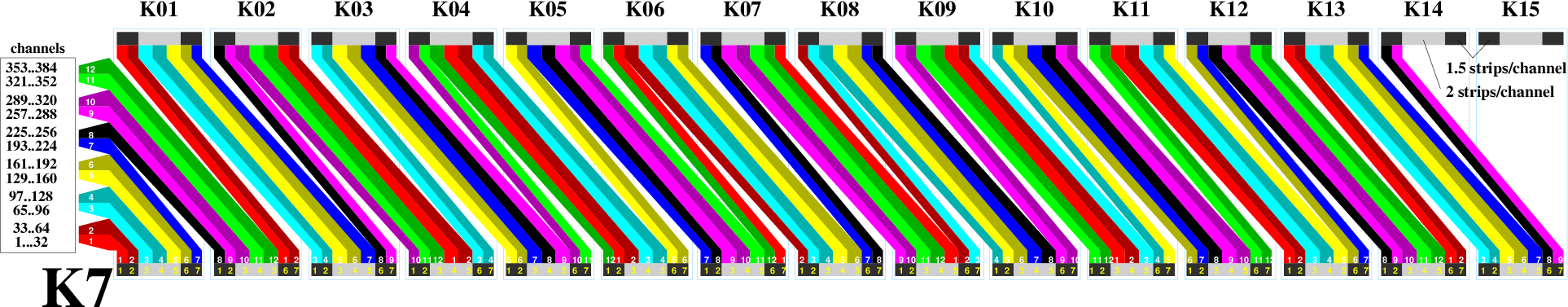 K5, K7 Upilex (PA fig. 4.11,4.12)
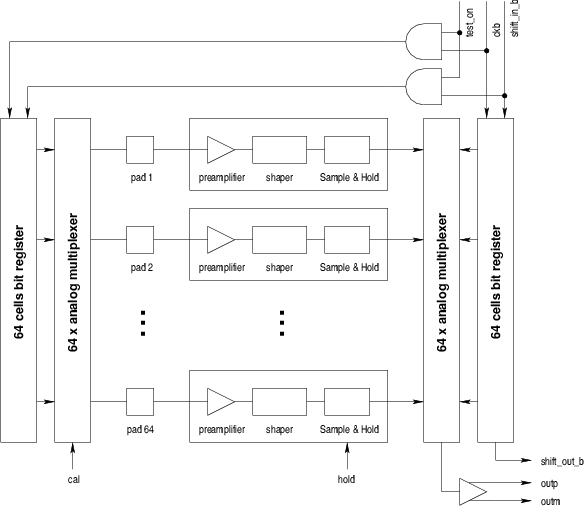
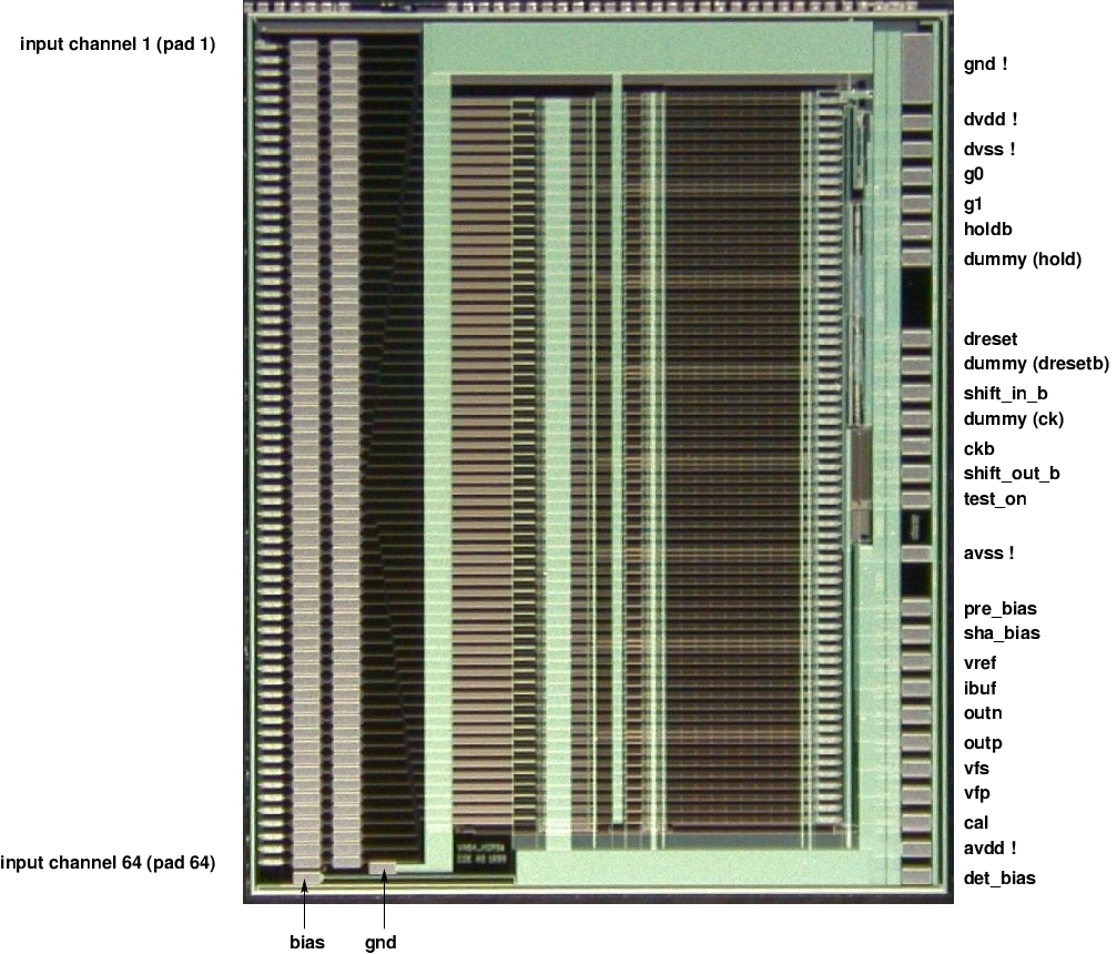 VA64hdr_9 (PA fig. 4.16, 4.17)
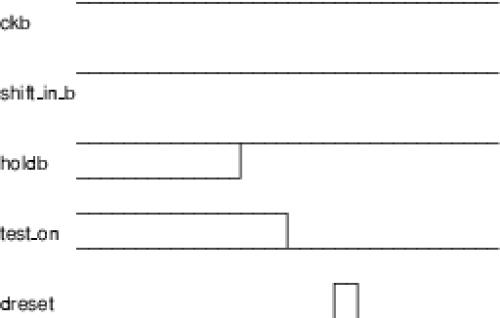
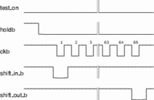
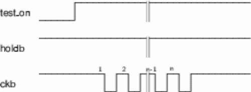 VA reset, readout and test sequence (PA tab. 4.5)
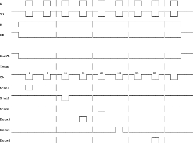 HCC control sequence (PA fig.4.18)
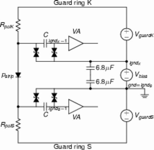
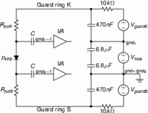 AMS-01 and AMS-02 biasing method (PA fig. 4.20)
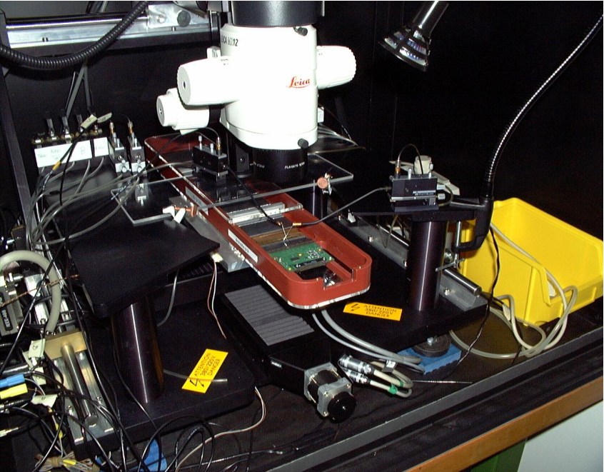
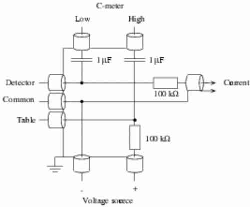
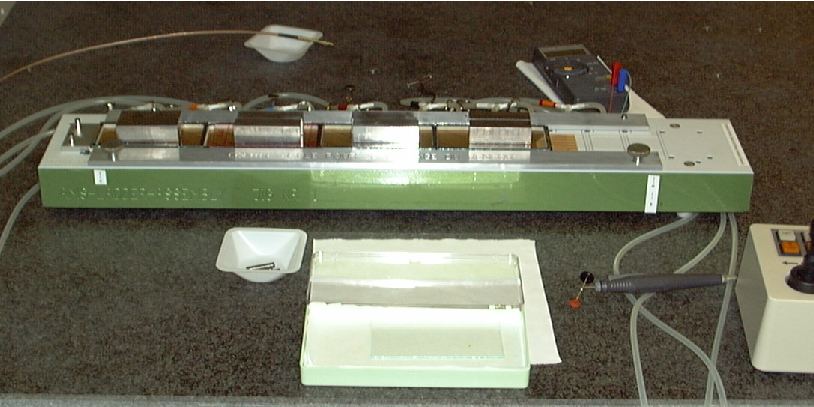
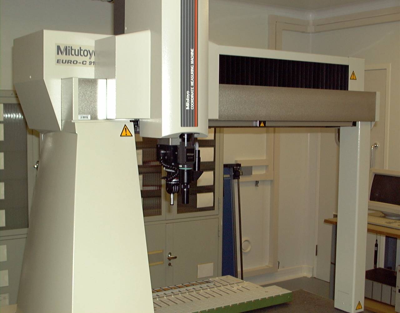
 Probe station (PA fig. 6.1-6.3)
 Sensor alignment precision (NIM fig. 2.60)
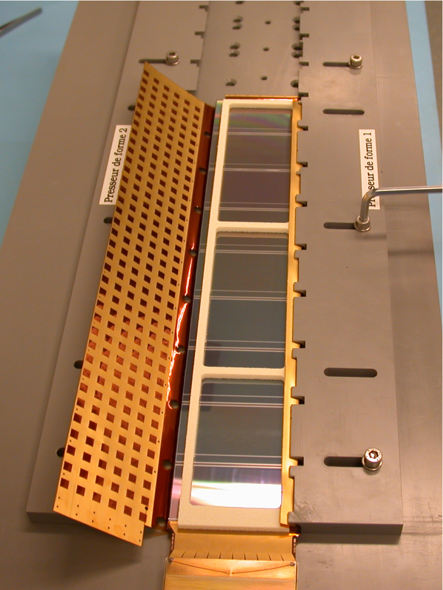
 Upilex gluing tools (PA fig. 5.4)
 Upilex gluing steps (PA fig. 5.5-5.7)
 Reinforcement gluing steps (PA fig. 5.8-5.13)
 K-hybrid gluing steps (PA fig. 5.14-5.16)

 S-hybrid gluing steps (PA fig. 5.17-5.20)

 Hybrid spacer and thermal grease (PA fig. 5.21-5.23)


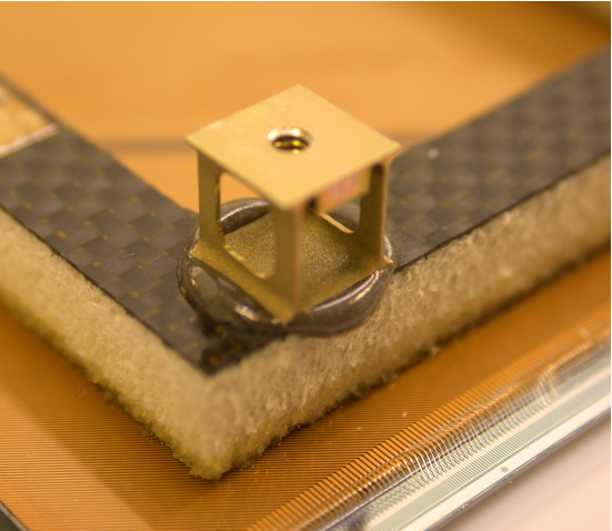
 Feet gluing steps (PA fig. 5.21-5.23)
 Spacer gluing and shield wrapping
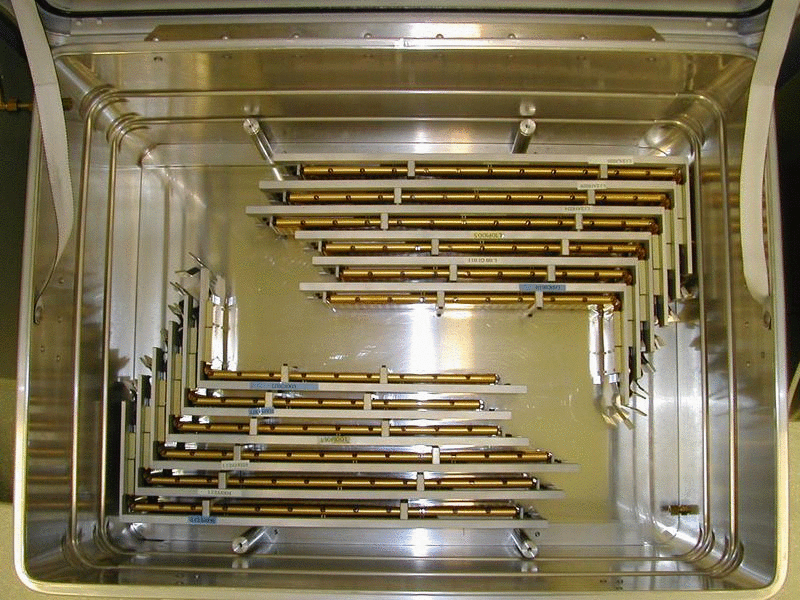
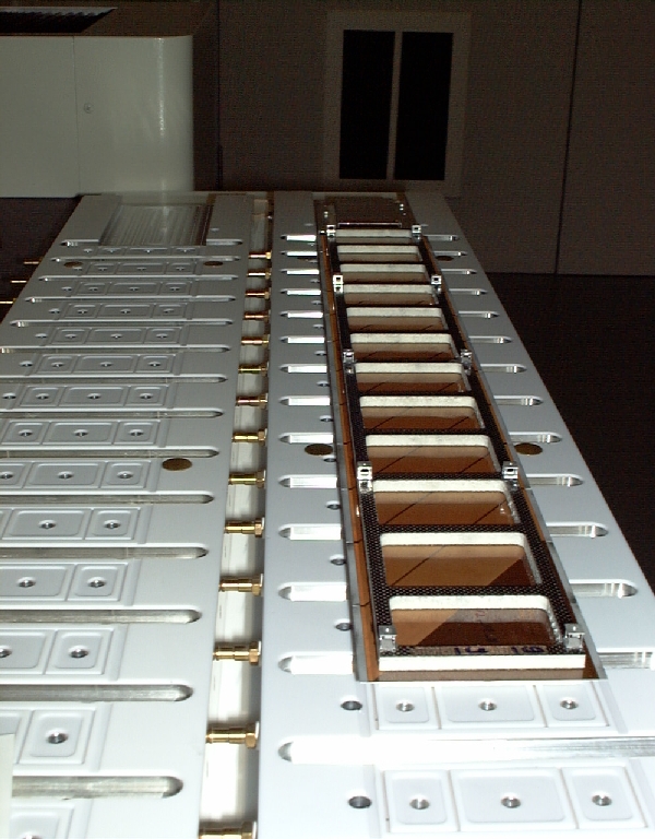
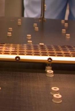
 Ladders ready for mount (NIM fig. 2.61)
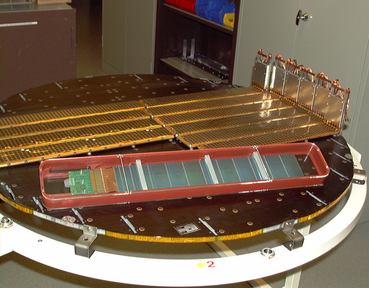 AMS-01 plane with AMS-02 ladder
 Odd layers longitudinal tolerance
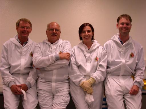 Geneva integration crew 2003
 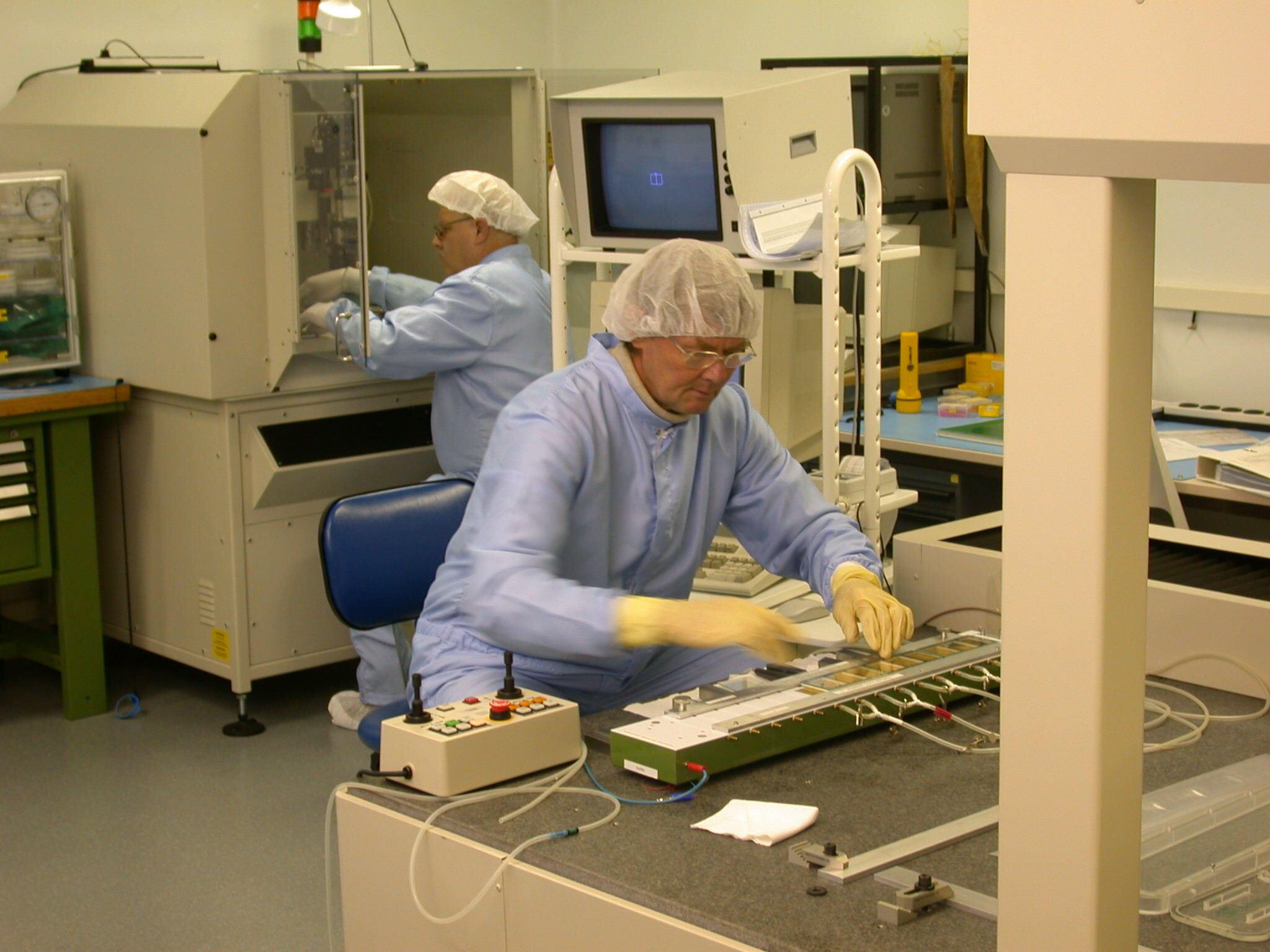 Geneva clean room

 Clean room equipment
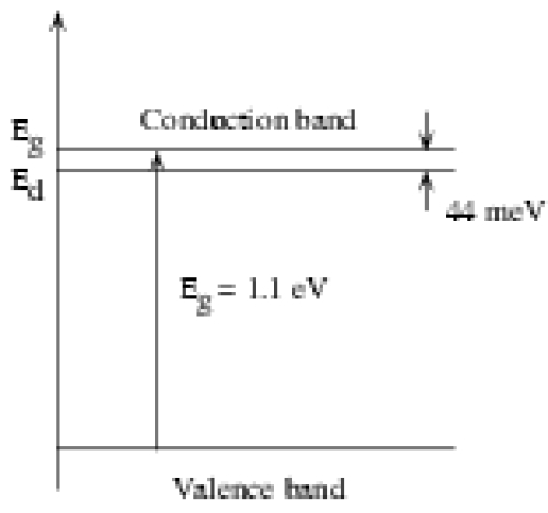
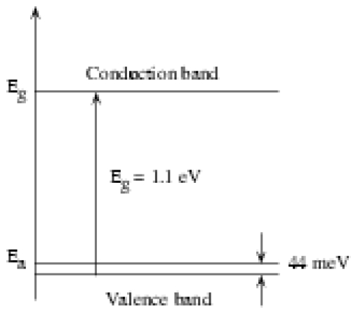
 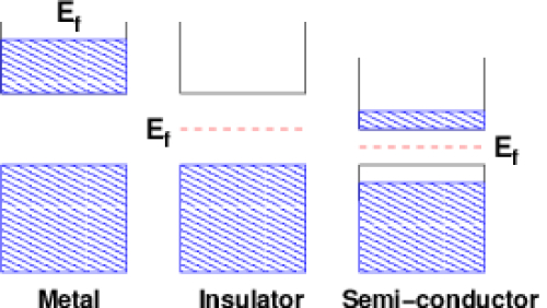 Band structure (PA fig. 3.1)
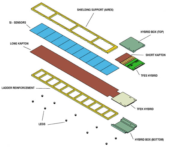
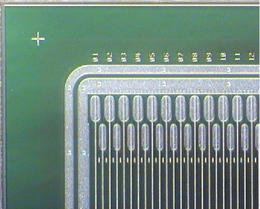
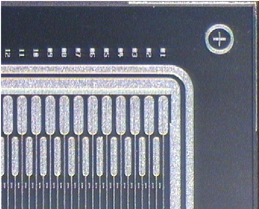
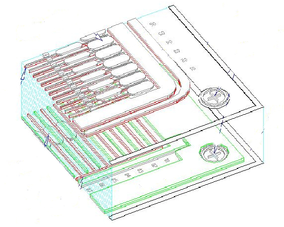
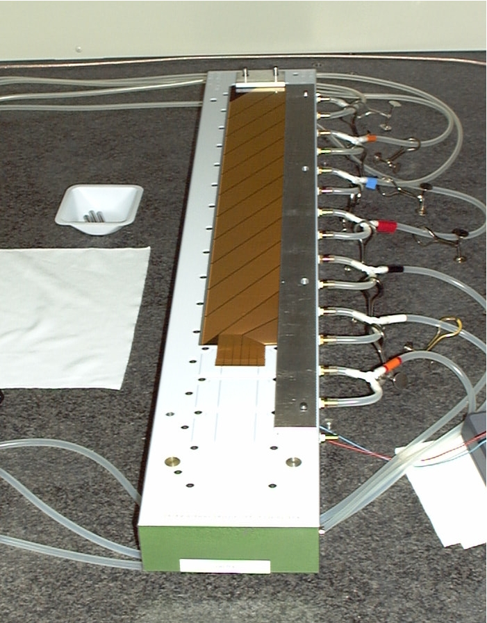
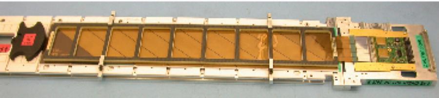
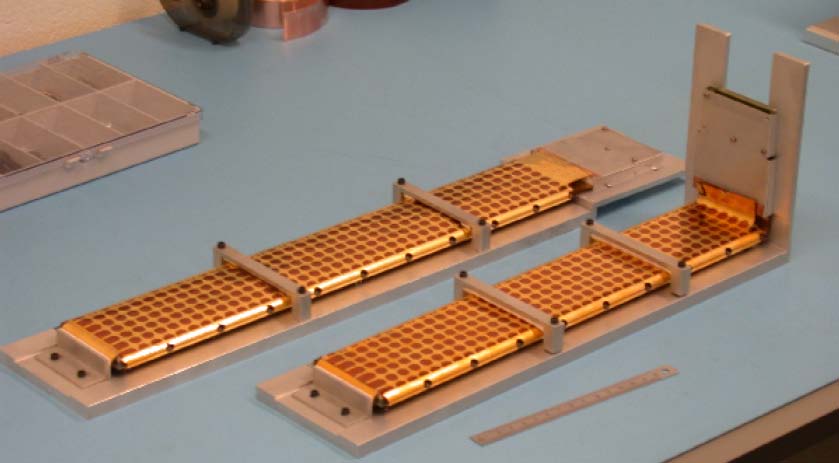
 Ladder exploded view
 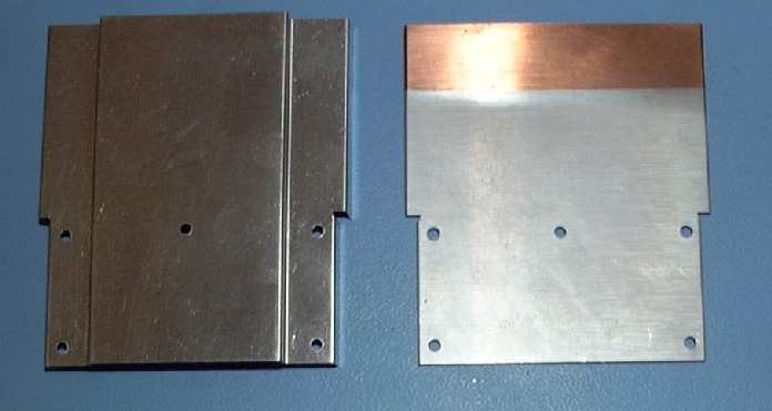 Hybrid box
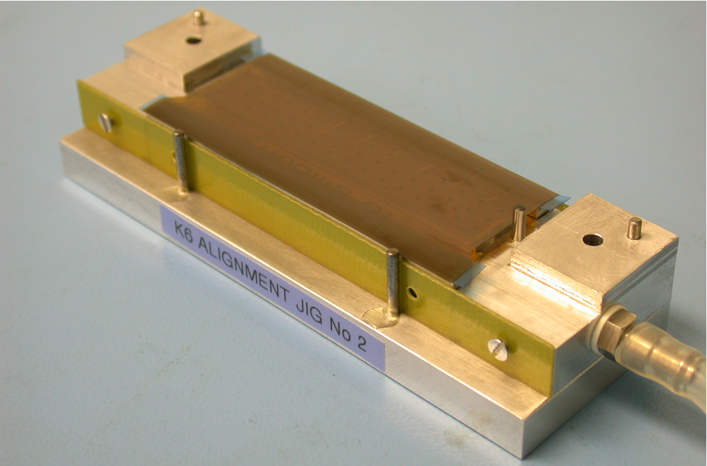
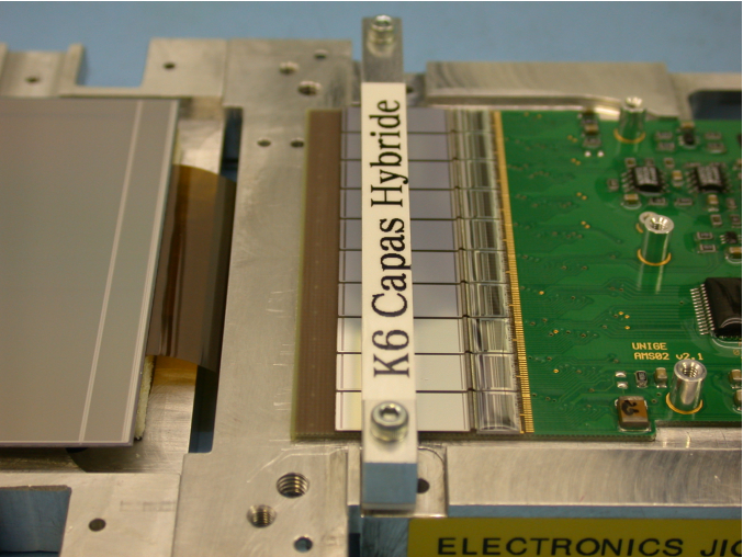
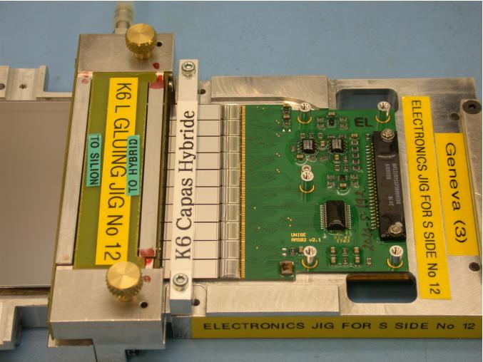
 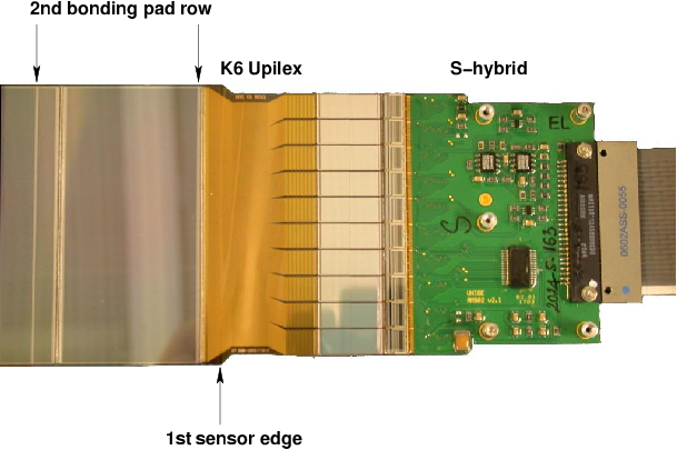 K6 Upilex (PA fig. 4.10)
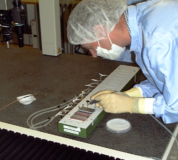
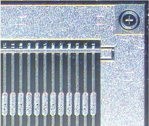
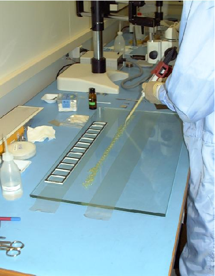
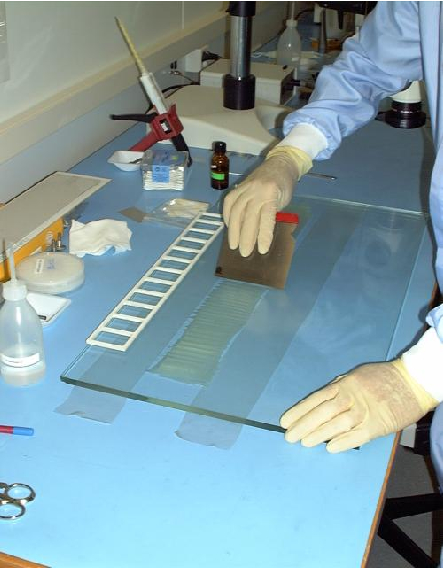
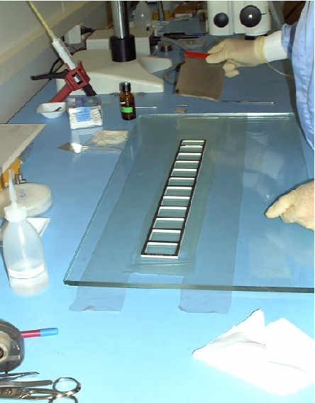
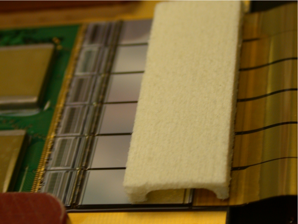
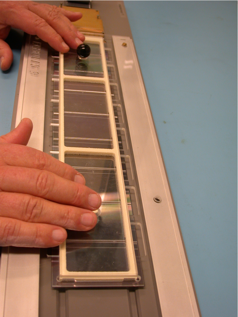
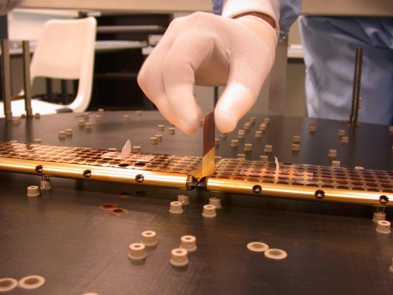
 Sensor positioning
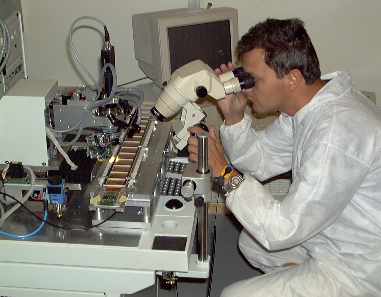
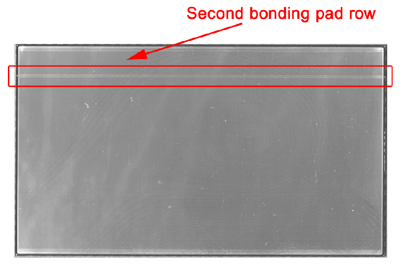
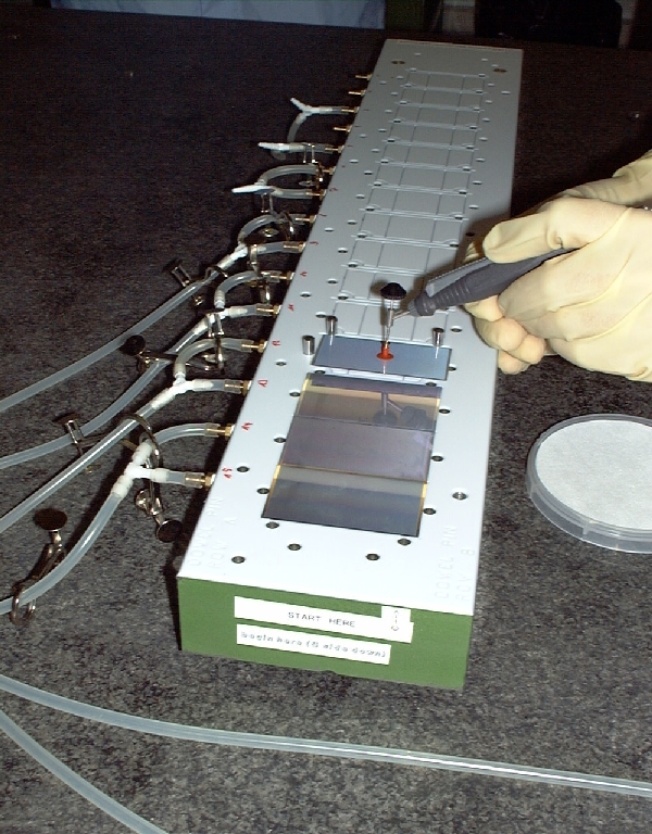
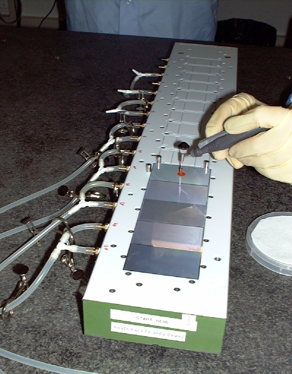
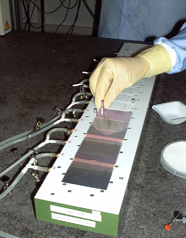
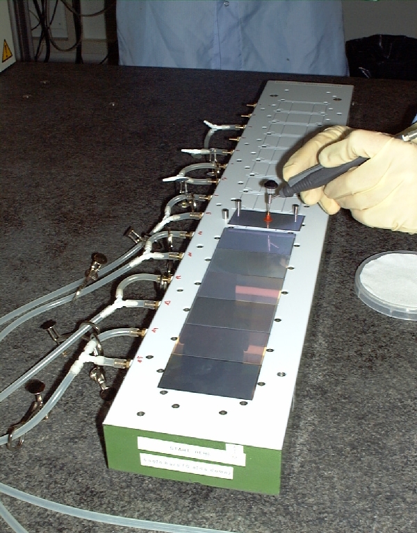
 Bonding at CERN
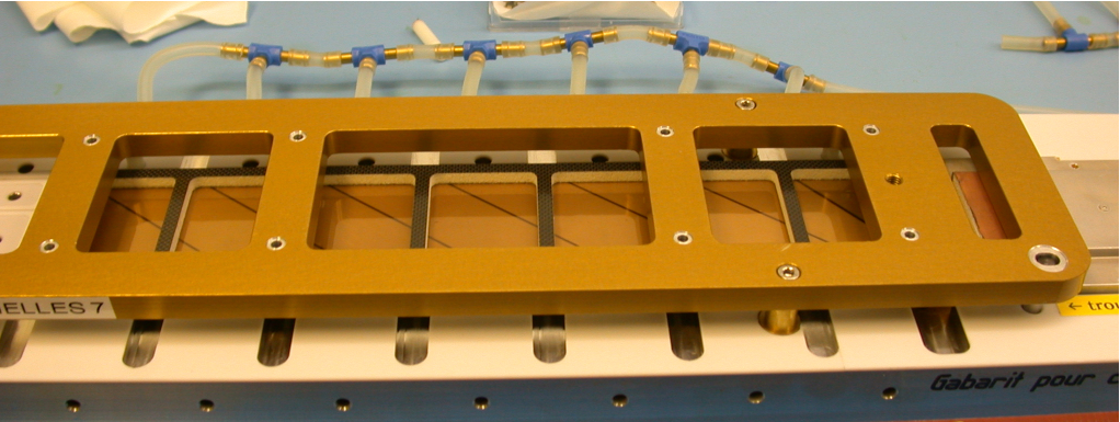
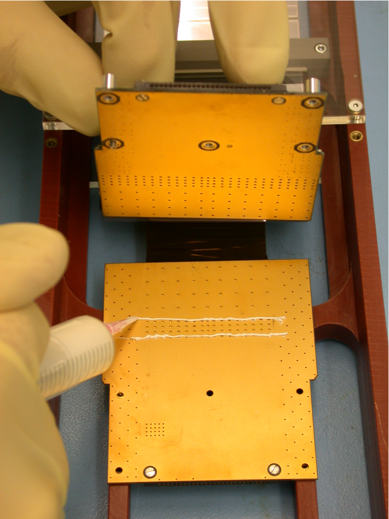
 Feet gluing
 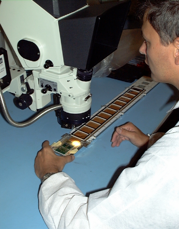 Hybrid gluing (by hand)
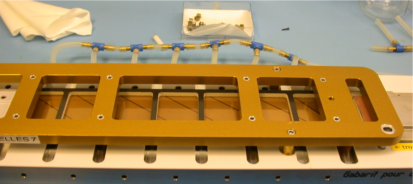
  Quarter plane vibration test
  Thermal bars
  Ladder fixation odd layers
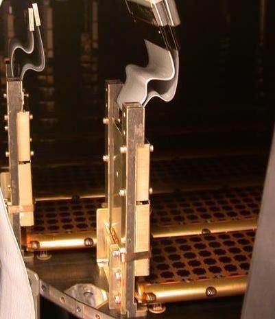
 Legs on even and odd layers
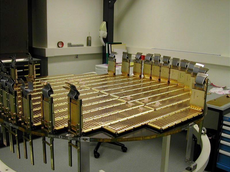
 Layer 2
  Layer 3
 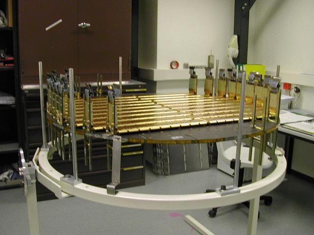 Layer 4
 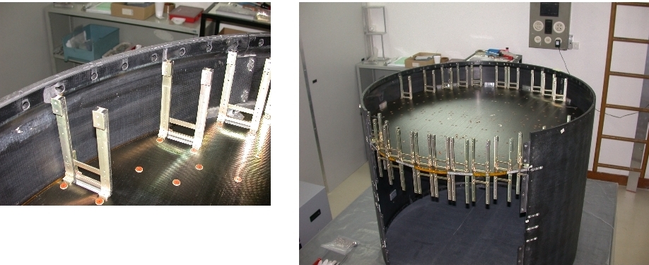 Tracker shell dry assembly
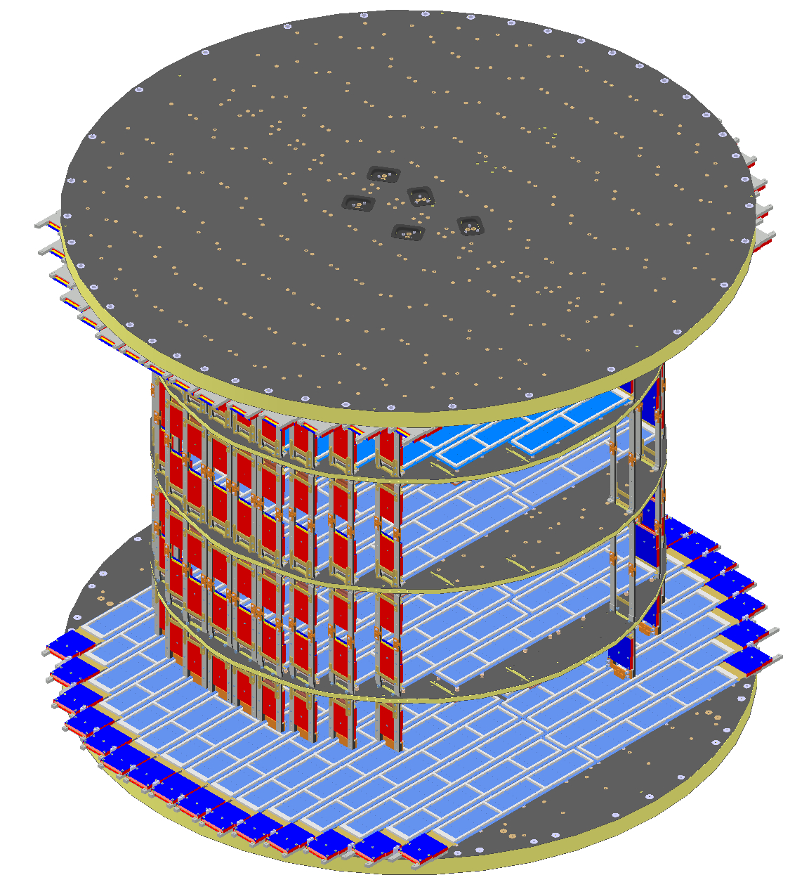

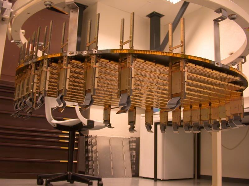
 Tracker model